
NIST’s layered photonics process brought more laser colors onto chips
The April research combined materials with different light-handling capabilities; mass production remained ahead.
- Event / announcement date
- 2026-04-15
- Earliest linked source date
- 2026-04-15
- NewsTumble first published
- 2026-10-25T22:14:43Z
- NewsTumble updated
- 2026-10-25T22:14:43Z
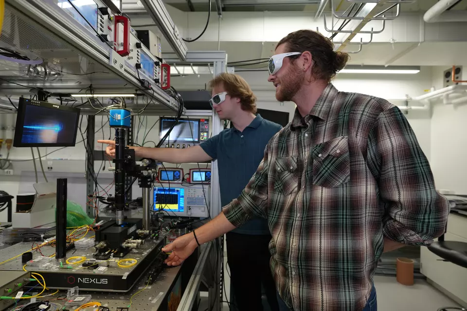
NIST scientists described a multilayer process for integrated photonics on April 15, 2026, combining materials that manipulate light in different ways. The work aimed to shrink lasers for optical clocks and quantum computers. It was a research advance, rather than a finished portable device. [1]
The starting structure combined silicon, glass and lithium niobate. Metal features supplied electrical control over color conversion and switching. The researchers then added tantalum pentoxide, also called tantala, which can convert a laser input into a wide range of visible and infrared wavelengths. [1]
Routing light between the layers joined those functions in one chip. Different atoms require specific laser wavelengths: compact semiconductor lasers cannot conveniently supply every color needed by quantum devices. Integrating conversion and control could reduce dependence on the bulky external equipment used in specialized laboratories. [1]
The agency described possible uses in sensing, navigation, computing and displays. The chips remained unready for mass production; a collaborating company was working on scaling. Demonstrating a fabrication route and generating colors on a chip should therefore be distinguished from proving manufacturing or field performance. [1]
The source
- National Institute of Standards and Technology: Any Color You Like: NIST Scientists Create Any Wavelength Lasers in Tiny Circuits for Light ↗
Source published 2026-04-15 · reviewed 2026-10-25
About this item: Retrospective source brief. No first-hand reporting or independent testing is claimed. Corrections policy.