
Glasslike bonding helped photonic chips survive a series of extreme tests
The March report preserved a key limit: direct high-temperature chip testing was not possible.
- Event / announcement date
- 2026-03-30
- Earliest linked source date
- 2026-03-30
- NewsTumble first published
- 2026-10-25T22:14:43Z
- NewsTumble updated
- 2026-10-25T22:14:43Z
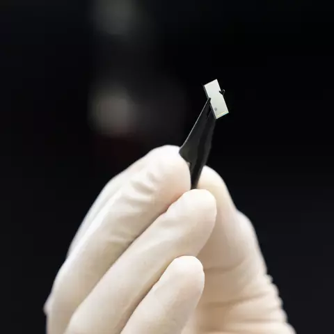
NIST reported a new packaging approach for photonic integrated circuits on March 30, 2026. Such chips carry information using light, but their optical-fiber connections can fail in demanding environments. The research focused on keeping that connection aligned and intact, not redesigning the entire chip. [1]
The team adapted hydroxide catalysis bonding, a method previously used in astronomical optical systems. A small amount of sodium hydroxide solution creates an inorganic, glasslike bond between surfaces. This replaces organic adhesives that can crack, release gases or degrade under cold, radiation, vacuum or heat. [1]
The packaged chip continued operating after cryogenic exposure, rapid temperature changes, ionizing radiation and vacuum tests. Commercial-fiber constraints prevented direct high-temperature testing of the packaged chip. Additional studies supported mechanical stability at high temperatures; that is narrower than a full operational chip test under those conditions. [1]
The bonding process still took several days. NIST described faster manufacturing as an engineering opportunity, not a production capability already demonstrated. Potential uses include space instruments, nuclear environments and quantum technology, without proving readiness for every mission or installation. [1]
The source
- National Institute of Standards and Technology: NIST Researchers Develop Photonic Chip Packaging That Can Withstand Extreme Environments ↗
Source published 2026-03-30 · reviewed 2026-10-25
About this item: Retrospective source brief. No first-hand reporting or independent testing is claimed. Corrections policy.